DanielVigna.com
← All notebooks
Notebook

SRAM compute-in-memory macro

A digital SRAM compute-in-memory macro in the ASAP7 7 nm PDK, laid out and verified with my own OpenLayout EDA flow.

  • 11 decisions
  • 1 measurement
  • 1 open
  • 2 tooling
Last entry Oct 16, 2026Started Oct 14, 2026

Now

  • Route b2SRAMsbc_INT8x8 (D10, D11): BL/BLB down the columns, Pk_k[7:0] to the bottom edge, WL / X per row; then DRC, LVS, connectivity.

  • Decide the reduction and accumulator: one fused carry-save tree (8 P bits per column plus the registered sum / carry fed back, one carry-propagate add at the end) vs. popcount, cross-column add and a ripple accumulator. Signed INT8: MSB complement plus a preloaded constant (weights); invert P and add 1 on the input's MSB cycle.

  • Bit-exact Python reference model of the 8-weight dot product before the adder schematics.

  • Target metric: energy per MAC (TOPS/W) at a stated throughput.

  • SRAMCIMsbc_INT8 still uses INVx1 (D11 replaced it in the 2-bit array).

  • Row testbench with PEX: write a weight, toggle XB, check P[7:0]; measure P rise/fall (D5) and the XB driver (D7).

  • Shift-accumulate adder from standard cells (16-bit, MSB-first).

  • Corners: SS/FF models and VDDV_{DD}/temperature sweeps for every delay and energy number.

  • Hierarchical PEX results (separate session), then redo M1.

How this notebook works

Every design decision and every measurement gets one entry, written when it happens and appended in date order. Each day starts a new heading, and every entry names the topic it touches (see Entries by topic at the end). The fields of an entry:

Question

what was being decided or measured.

Options

the alternatives considered.

Method

tool, testbench, corner, and the script or file that reproduces it.

Result

the numbers.

Decision

what was chosen and why.

Revisit if

the condition that would reopen it.

Claims that are reasoning but not yet measured are marked to verifylike this. Scripts live in scripts/, raw data in data/, next to this file (~/papers/notebook/sram-cim on the VM).

Setup (all entries unless noted).ASAP7 predictive 7 nm PDK; OpenLayout flow (xschem, KLayout, FasterCap PEX, ngspice with BSIM-CMG); SRAM-Vt devices (nmos_sram, pmos_sram) in the bitcell; TT models (7nm_TT.pm), VDD=0.7V_{DD} = 0.7 V. Gate pitch (CPP) 54 nm, cell height 270 nm (one 7.5-track standard-cell row).

Entries

Newest first
5 entriesD8D9D10D11T2
D8DecisionArchitecture

Back to the 2-bit cell: a 4-row array of 8 INT8 weights

Question

With the dataflow understood (D1), which cell and array shape does the signed INT8 design use?

Options

(a) stay with the 1-bit 10T cell (D4); (b) the 2-bit cell b2SRAMsbc (D3), 8 cells per row, 4 rows.

Method

Reasoning on the mapping, then the schematic b2SRAMsbc_INT8x8.sch, netlisted with xschem (32 cells; a script checked that every cell sits on the WL / XB / P / BL nets of its row and bit).

Result

Each cell holds bit jj of two weights (latch 1 and latch 0, sharing BL/BLB). Row rr holds W2r+1W_{2r+1} (WL[2r+12r{+}1], XB[2r+12r{+}1], P2r+1_{2r+1}[7:0]) and W2rW_{2r} (WL[2r2r], XB[2r2r], P2r_{2r}[7:0]); 4 rows ×\times 8 cells = 64 bits = 8 weights, BL[jj]/BLB[jj] shared down each column. Every NOR computes in the same cycle, so each bit column delivers 8 product bits per cycle: the column sum is an 8-input popcount (compressor tree), not a single add. The dot product ∑i=07WiXi\sum_{i=0}^{7} W_i X_i of 8 signed 8×88\times8 terms needs 8+8+3=198+8+3 = 19 bits (worst case 8⋅(−128)(−128)=2178 \cdot (-128)(-128) = 2^{17}). Area: 0.102 μm20.102\,\mu\text{m}^2 per bit vs. 0.1460.146 for the 10T cell.

Decision

(b). D4's reason (the 2-bit mapping was hard to reason about) no longer holds, and the 2-bit cell is 30% smaller per bit.

Revisit if

the shared bitlines complicate writes, or read disturb (D6) shows up in simulation.
D9Decision1 to verifyBitcell

b2SRAMsbc NOR pMOS: 2 fins

Question

Apply D5 to the 2-bit cell, whose NOR was p1/n2.

Options

Widen the four NOR pMOS (M13, M14, M17, M18) to 2 fins in the existing 14-CPP placement, or re-place the cell.

Method

Schematic nfin 1→21 \rightarrow 2; in the layout only the PCell parameter nfin of those four instances (second fin on fin row 7, ACTIVE / LISD / SDT down to 189 nm). Each widened device shares diffusion with a 1-fin latch pMOS, so the ACTIVE steps from 2 to 1 fin at the shared contact (DRC allows it). KLayout DRC, LVS, OpenLayout connectivity check.

Result

LVS match. The wider LISD came 10 nm from three LIG gate contacts (LIG–LISD/SDT spacing ≥14\ge 14 nm, corner ≥15\ge 15): two were moved down 5 nm; the third, wedged between the Q_bar[1] LISD strap and the new LISD, was trimmed to 177177–207×144207 \times 144–174174 nm, which keeps its LIG tip-to-side spacing at exactly 25 nm. DRC clean, LVS match, no shorts or opens. Cell size unchanged (14 CPP ×\times 270 nm).

Decision

2/2 (p2/n2): the pull-up is no longer the 4×4\times slower edge to verifyP rise/fall on the PEX row. The nMOS stay at 2 fins because the N row is one 2-fin chain.

Revisit if

the P rise is still the slow edge after PEX.

D10DecisionArray

Array assembly: on the fin grid, bus pins

Question

How are the 32 cells placed and pinned?

Method

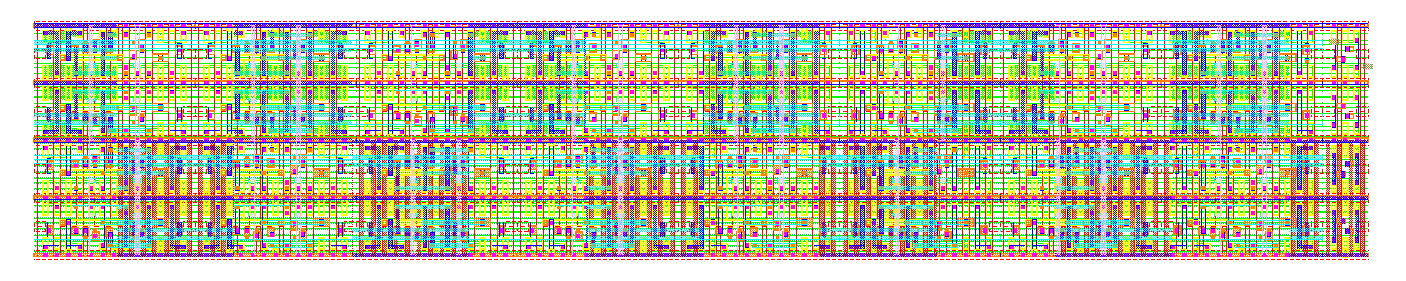
Rows alternate unmirrored / mirrored about xx so neighbours share a rail (VSS at 270 and 810 nm, VDD at 540 nm); 14-CPP column pitch (756 nm). DRC of the assembled layout. Symbol b2SRAMsbc_INT8x8.sym, checked by netlisting an instance (96 bus bits, instance and subcircuit in the same order).

Result

The first placement put the rows at y=20,290,…y = 20, 290, \ldots nm and every fin failed FIN.S.1: the fin grid is absolute (fin centrelines at 13.5+27k13.5 + 27k nm from the layout origin), so a row origin must be a multiple of 27 nm. Moving the array by −20-20 nm cleared all 40 violations; every instance was already on the exact pitch. The symbol has 12 bus pins: BLB[7:0], BL[7:0] (top), WL[7:0], X[7:0] (left), P7[7:0] … P0[7:0] (right); the schematic's per-bit BL/BLB/WL pins became labels plus bus pins so symbol and schematic match.

b2SRAMsbc_INT8x8 layout on 2026-10-16 (routing in progress): 4 rows × 8 b2SRAMsbc, rows mirrored in pairs to share rails, one DRIVE2b at the right end of each row; 6.26 × 1.08 m.
b2SRAMsbc_INT8x8 layout on 2026-10-16 (routing in progress): 4 rows ×\times 8 b2SRAMsbc, rows mirrored in pairs to share rails, one DRIVE2b at the right end of each row; 6.26×1.08 μm6.26 \times 1.08\,\mu\text{m}.
Decision

Row origins on multiples of 27 nm (the 270 nm row pitch keeps them there); bus pins only.

Revisit if

the array is placed inside a larger block: its origin there must also be a multiple of 27 nm in yy (and of 54 nm in xx).

D11Decision1 to verifyRow

DRIVE2b: one dual-inverter drive cell per row

Question

Each row needs XB for two weights; two separate INVx1 cells (3 CPP each) sat at the row end.

Options

(a) two INVx1, 6 CPP; (b) one cell, two inverters sharing their VDD / VSS source column, 4 CPP.

Method

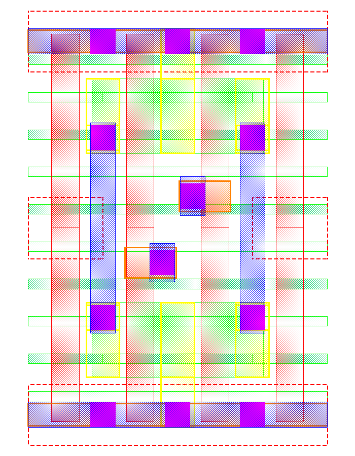
New cell DRIVE2b (schematic, symbol with A[1:0] / Z[1:0], layout from OpenLayout PCells: inverter 0 mirrored about the shared source column at x=108x = 108 nm, gates at 81 and 135 nm, outputs Z[0] / Z[1] on M1 at 54 / 162 nm, input contacts staggered in yy). Each half keeps the INVx1 sizing (p2/n2, SRAM-Vt). DRC, LVS, connectivity check; DRC of a 4×44\times4 block of DRIVE2b in every row mirroring and left/right flip.

Result

4 CPP ×\times 270 nm =0.058 μm2= 0.058\,\mu\text{m}^2 vs. 0.0870.087 for two INVx1 (−33%-33\%, 108 nm shorter per row). DRC clean, LVS match, and the 4×44\times4 block is clean: the cell is symmetric about its source column, so any flip keeps the sources on the shared rails. With two INVx1, flipping one row's inverters left/right had put an output LISD 18 nm from the next row's source LISD at the shared rail (LISD tip-to-tip ≥27\ge 27 nm). Swapped into the array in place of the 8 INVx1 (instances x39, x49, x59, x69).

DRIVE2b, 4 CPP × 270 nm: VSS rail (bottom) and VDD rail (top), shared source column in the middle, outputs Z[0] / Z[1] on the M1 verticals at the edges, the two staggered input contacts between them.
DRIVE2b, 4 CPP ×\times 270 nm: VSS rail (bottom) and VDD rail (top), shared source column in the middle, outputs Z[0] / Z[1] on the M1 verticals at the edges, the two staggered input contacts between them.
Decision

(b). XB[ii] still drives 8 NORs: 8×(2+2)=328 \times (2 + 2) = 32 fins from a 4-fin input, FO ≈8\approx 8 plus wire to verifyXB edge rate on the PEX row; D7's two-stage option if too slow.

Revisit if

the XB edge limits the cycle, or a row needs more than two inputs.

T2ToolingTooling

Tooling notes from assembling the array

Editing an OpenLayout layout in a batch script without the OpenLayout_ASAP7 PCell library registered saves the transistors as static cells: LVS still passes, but the connectivity view computes terminals from default PCell parameters and reports false shorts (and chain flags such as abut_left can silently change). Batch edits must register the library and change PCell parameters, not shapes. M4–M7 are SADP layers on absolute routing tracks: a minimum-width M4 wire (24 nm) must have its lower edge at an odd multiple of 24 nm (48 nm pitch). Wanted next: a pin-placement tool (the array has 96 pin bits; placing them by hand is slow) and lighter KLayout highlighting while moving many instances (it loads the GPU heavily).

9 entriesD1D2D4D5D6D7O1M1T1
D1DecisionArchitecture

Dataflow: weight-stationary, bit-serial input

Question

How does an array of 1-bit AND cells compute a multiply?

Options

(a) 8 parallel input bits per row (bitwise AND only); (b) one input bit per row per cycle, broadcast to all weight bits (bit-serial).

Method

Reasoning; worked example below.

Result

Each cell computes P=Q‾+X‾‾=Q⋅XP = \overline{\overline{Q} + \overline{X}} = Q \cdot X. With (a) a row yields WiXiW_i X_i for matching bits only, which is not a product. With (b) a row holding weight WW yields the partial product W⋅x[t]W \cdot x[t] each cycle, and

W×X=∑t=072t (W⋅x[t]),MSB first: Acc←2 Acc+P.W \times X = \sum_{t=0}^{7} 2^t\,(W \cdot x[t]), \qquad \text{MSB first: } \mathrm{Acc} \leftarrow 2\,\mathrm{Acc} + P.

Example (4 bit): W=11012=13W = 1101_2 = 13, X=01102=6X = 0110_2 = 6: Acc =0,13,39,78=13×6= 0, 13, 39, 78 = 13 \times 6. With several rows, the PP bits of each column are summed first (popcount), giving ∑iWi xi[t]\sum_i W_i\,x_i[t] per cycle; the same accumulator then forms the dot product ∑iWiXi\sum_i W_i X_i.

Decision

(b). The weight stays in the SRAM and the input streams past it; a row is one reused row of AND gates of an array multiplier.

Revisit if

throughput needs more than one input bit per cycle (e.g. 2-bit-serial inputs).

D2DecisionArchitecture

Start with one 8×\times1 row, not a full array

Question

What is the first block to build and verify?

Options

(a) the full multi-row array with column adders; (b) a single row of 8 cells plus a shift-accumulate adder (an 8×88\times8 bit-serial multiplier).

Decision

(b). It exercises the cell, the NOR and the accumulator with nothing to add across rows; more rows later only insert per-column adders between the row and the accumulator.

Revisit if

n/a (staging decision).

D4DecisionBitcell

1-bit 10T cell instead of the 2-bit cell

Question

Use the dense 2-bit cell, or a simpler 1-bit cell (6T + one NOR2)?

Options

(a) b2SRAMsbc: two latches share BL/BL_Bar, selected by WL[1]/WL[0]; (b) SRAMCIMsbc: one latch, one NOR.

Method

Layout in OpenLayout; DRC and LVS (data/cells/); bounding box via scripts/bbox.rb.

Result

SRAMCIMsbc: 10 CPP ×\times 270 nm =0.146 μm2= 0.146\,\mu\text{m}^2 per bit, DRC clean, LVS match. That is +43%+43\% area per bit vs. (a).

Decision

(b). The 2-bit array's mapping (two weights interleaved per cell row, shared bitlines) made the design hard to reason about; the 1-bit cell keeps one cell = one weight bit while the dataflow is being learned.

Revisit if

area becomes the main metric, or once the 1-bit design works end to end (the 2-bit cell is "two 1-bit cells stacked", so the architecture carries over).

D5Decision1 to verifyBitcell

NOR2 sizing

Question

Fin counts of the NOR's series pMOS and parallel nMOS.

Options

p1/n2 (as in b2SRAMsbc); 2/2; p2/n1.

Method

RC reasoning relative to a 1-fin inverter, assuming similar drive per fin for n and p in ASAP7 to verifyper-fin IonI_{on} of nmos_sram vs. pmos_sram at TT.

Result

Pull-up of two series devices vs. worst-case pull-down of one device: p1/n2 ⇒\Rightarrow rise ≈4×\approx 4\times slower than fall; 2/2 ≈2×\approx 2\times; p2/n1 ≈\approx balanced. The slow edge is PP rising (Q=1Q=1, X=1X=1), which sets the compute delay. Extra nMOS fins only add gate load on the storage node and on XB.

Decision

p2/n1 in SRAMCIMsbc.

Revisit if

the measured rise/fall from the PEX row testbench disagrees, or the N chain forces 2-fin nMOS.

D6Decision1 to verifyBitcell

Latch sizing and read path

Question

PU/PG/PD = 1/2/2 fins gives a cell ratio β=1\beta = 1; is that safe?

Result

A classic bitline read with β=1\beta = 1 risks read disturb to verifyread SNM at TT. The CIM cell does not need bitline reads: driving X=1X = 1 shows the stored bit on PP, and the NOR loads the storage node with gate capacitance only.

Decision

Keep 1/2/2; read through the NOR, no sense amplifiers.

Revisit if

a conventional SRAM read mode is wanted.

D7Decision1 to verifyRow

XB driver: INVx1

Question

Which inverter drives the row's XB line?

Options

INVxp67 (2+2 fins), INVx1 (3+3), INVx2 (6+6) from asap7sc7p5t_28_R.

Method

Load per cell: NOR nMOS 1 fin + pMOS 2 fins = 3 fins; 8 cells = 24 fins, plus ≈0.17\approx 0.17 fF of XB wiring per cell (PEX). Electrical fanout = load / input fins.

Result

INVx1: FO ≈4\approx 4–5. INVx2: FO ≈2\approx 2–2.5 but doubles the load on the stage driving it. The inverter also produces XB from the true input bit, and the 270 nm standard-cell height matches the bitcell, so it can abut the row.

Decision

INVx1 to verifyXB edge and P delay with INVx1 vs. INVx2 on the 1×\times8 PEX row.

Revisit if

XB fans out to more weights (an 8×88\times8 matrix: 64 cells, ≈\approx190 fins, FO ≈32\approx 32 for INVx1 ⇒\Rightarrow two-stage buffer, e.g. INVx1 →\rightarrow INVx4).

O1OpenRow

Row schematic status (SRAMCIMsbc_INT8)

WL and BL[7:0]/BLB[7:0] wired (x1 = bit 7). Open: XB tied to one net with an ipin; P labelled P[7:0] with an opin. Symbol: XB (left) and P (right) share y=10y = 10, which shorts Pk_k to XBk+1_{k+1} on abutment; plan: XB pass-through on both edges, P on the bottom edge, matched in layout.

M1MeasurementVerification

Flat PEX and SPICE scaling

Question

How large an array can be extracted and simulated flat overnight (≤8\le 8 h)?

Method

SRAMCIMsbc tiled 1×81\times8 and 2×82\times8 (scripts/tile.py: 0.54 μ\mum pitch, odd rows mirrored); openlayout pex (FasterCap 3D); 12 ns ngspice transient (scripts/tb_*.sp). VM: 8 vCPU, 10 GB RAM. Raw: data/pex-scaling/.

Result
LayoutCellsConductorsFasterCap (s)Memory (GB)Capacitorsngspice (s)
1 cell1163.30.462220.85
1×81\times881073220.503 68437.8
2×82\times8161979711.0217 662failed†^\dagger

†^\dagger operating point failed; the tiles were not wired as a real array, so treat as order-of-magnitude.

FasterCap time grows roughly as (conductors)1.8–2.3(\text{conductors})^{1.8\text{--}2.3}; capacitor count roughly quadratically. Extrapolated: ≈\approx1 300 conductors (≈\approx100 cells) fit in 8 h at ≈\approx6–7 GB; 640 weights ×\times 8 bits (≈\approx5 000 cells, ≈\approx30 000 conductors) would take months and >>100 GB.

Decision

Never extract or simulate the full array flat. Verification ladder: (1) leaf-cell PEX, reused per instance; (2) critical paths with PEX: one row with full WL/XB load, one column with full BL load, the adder's slowest path; (3) function by a behavioral model (Python/Verilog) of the whole array on the full dataset.

Revisit if

hierarchical PEX lands in OpenLayout (in progress), which changes the cost of step 2.

T1ToolingTooling

OpenLayout/xschem fixes found while designing

Symbol pins off the 10 grid (the symbol editor's 2.5 snap) could not be reached by schematic wires: pins now move on 10 when selected, and saving a symbol snaps strays (stubs kept straight, one undo). Copying several objects with c + a click on the selection kept only one: xschem's cadence-compat release trimmed the selection on command clicks. Fixed with xschem patches; OpenLayout commit dc53d6b.

1 entryD3
D3DecisionBitcell

2-bit cell placement (b2SRAMsbc), 14 CPP

Question

Smallest placement of the 20-device 2-bit CIM cell (two 6T latches, two NOR2).

Options

Original N/P/N frame, 16 CPP ×\times 405 nm; N/P frame at 270 nm height.

Method

Euler-path chaining: 6 odd-degree P nets ⇒\Rightarrow at least 3 P chains ⇒\Rightarrow 14 CPP minimum; every P gate column shares poly with an N gate of the same net. Unchained transistors keep LISD two gate pitches apart (double diffusion break). KLayout DRC.

Result

14 CPP ×\times 270 nm, −42%-42\% area vs. the original, DRC clean; later routed to M3, DRC clean, LVS match. 0.756×0.27 μm=0.204 μm20.756 \times 0.27\,\mu\text{m} = 0.204\,\mu\text{m}^2, i.e. 0.102 μm20.102\,\mu\text{m}^2 per bit.

Decision

Kept as the dense reference point (superseded for now by D4).

Rendered from sram-cim/notebook.tex on GitHub; synced Oct 21, 2026, 11:52 PM CDT.